Contents
- What is Solder Resist and Its Core Functions?
- Solder Resist Application Process: A Multi-Step Approach
- Types of Solder Resist Materials
- Negative vs. Positive UV Exposure
- The Significance of Solder Resist Color and Thickness
- Environmental Considerations and Compliance
- Conclusion
- Mustar: A Leading Turnkey PCBA Manufacturer Management Systems
Solder resist, widely known as solder mask, is a fundamental protective polymer coating applied to Printed Circuit Boards (PCBs). While both terms are used interchangeably, “solder resist” is arguably more technically precise, as it describes the material’s function of resisting molten solder during assembly. Regardless of nomenclature, its presence is paramount in ensuring the reliability and performance of modern electronic devices.
What is Solder Resist and Its Core Functions?
At its essence, solder resist is a thin layer of protective polymer applied over copper traces on a PCB, strategically leaving exposed only the pads and vias where solder connections are required. Its primary objective is to prevent molten solder from bridging adjacent conductors, thereby averting unwanted electrical shorts.
The key functions of solder resist include:
-
Preventing Short Circuits: The most critical role, ensuring solder adheres only to designated areas.
-
Protecting Circuit Patterns: Safeguarding copper traces from environmental elements like dust, heat, and moisture, which can degrade performance over time.
-
Supporting Manufacturing/Smooth Manufacturing Process: Facilitating automated assembly by defining precise soldering areas, preventing solder from spreading uncontrollably.
-
Maintaining Electrical Insulation: Ensuring that different circuit patterns remain electrically isolated, crucial for proper circuit operation.
Solder Resist Application Process: A Multi-Step Approach
The application of solder resist is a precise multi-stage process.Learn more about our high-precision PCB manufacturing processes at Mustar:
-
Surface Preparation: Thorough cleaning of the bare PCB to remove contaminants like dust or oxidation.
-
Solder Mask Application: Depending on the material type, this involves:
-
Epoxy: Screen printed.
-
Liquid Photoimageable (LPI): Sprayed or curtain coated.
-
Dry Film: Laminated onto the board.
-
-
UV Exposure (for LPI and Dry Film): A photographic film with the circuit image is overlaid. UV light polymerizes (cures) the exposed areas, defining the solder mask openings.
-
Development: Unexposed (uncured) areas are washed away using a developer solution, revealing the pads and vias intended for soldering.
-
Thermal Curing: A final baking step hardens and fully cures the solder mask, making the PCB ready for subsequent assembly stages.
Types of Solder Resist Materials
Different applications and manufacturing needs dictate the choice of solder resist material:
-
Liquid Solder Resist: The most common and cost-effective type, applied by spraying or screen printing. Suitable for general purposes but with lower resolution for fine-pitch designs.
-
Dry Film Solder Resist: A laminated material offering excellent edge definition, often used in high-frequency (RF) PCBs.
-
Photo-sensitive Solder Resist: Specifically designed to react to UV light, making it ideal for intricate and high-density PCB designs. This category includes LPI, which is prevalent.
Negative vs. Positive UV Exposure
The photolithographic process can utilize two types of UV exposure:
-
Negative UV Exposure: Exposed areas harden and remain on the PCB, while unexposed areas are removed. This is the most common method for solder mask fabrication, especially for fine traces and delicate features.
-
Positive UV Exposure: Exposed areas become soluble and are washed away, while unexposed areas remain. This method is typically used for high-precision photolithography for circuit patterning, rather than solder masks themselves.
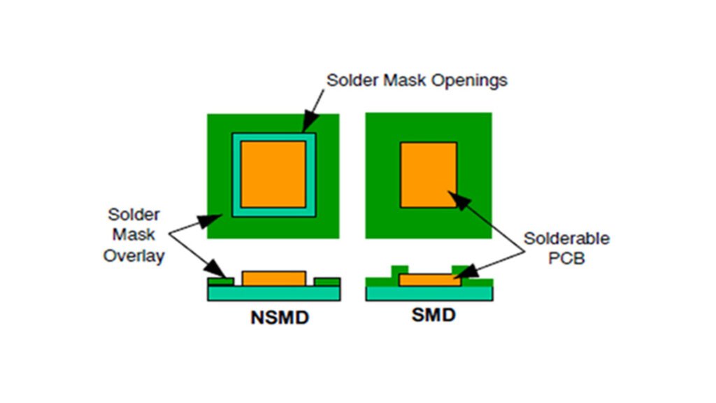
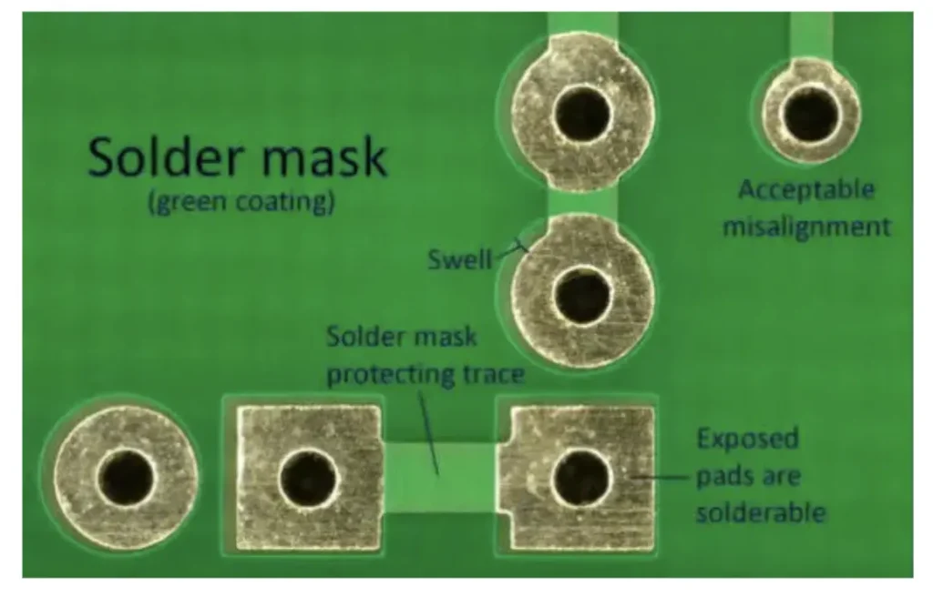
The Significance of Solder Resist Color and Thickness
Beyond aesthetics, the color and thickness of solder resist play functional roles:
-
Color: While green is historically preferred due to its high visibility under UV light (aiding photolithography and Final Quality Check (FQC) for defects), other colors like blue can enhance UV light accuracy for high-resolution applications. Some colors might also offer better thermal conductivity for high-power circuits.
-
Thickness: Typically ranging from 16 to 30 micrometers (or as thin as 0.3 mils), an optimal thickness is crucial. Too thin, and it can peel; too thick, and it can lead to component misalignment and soldering errors, requiring more solder paste. Thickness can also vary, often being thinner near trace edges.
Environmental Considerations and Compliance
Modern solder resist materials adhere to strict environmental standards:
-
RoHS (Restriction of Hazardous Substances): Ensures materials are lead-free and compatible with lead-free soldering processes.
-
REACH Compliance: Verifies the absence of dangerous compounds, complying with European Union regulations.
Conclusion
Solder resist is far more than a cosmetic layer; it is an indispensable component of PCB functionality and durability. From preventing short circuits and offering environmental protection to streamlining the manufacturing process, its role is pivotal. Understanding the various types, application methods, and material properties is key to achieving high reliability and low failure rates in the increasingly complex world of electronics manufacturing.
Mustar: A Leading Turnkey PCBA Manufacturer
Mustar (MU STAR Industry Co., Ltd), established in Shenzhen, China in 1998, has emerged as a TOP 1 PCBA manufacturer. With over 25 years of experience and a global presence in 98 countries, Mustar provides comprehensive turnkey solutions encompassing PCB manufacturing, component sourcing, and PCBA assembly.
Core Strengths & Capabilities:
-
Comprehensive Services: Offering end-to-end support from 1-64 layer PCB manufacturing and advanced PCBA assembly (supporting intricate components like 01005, BGA, QFN) to professional electronic component sourcing.
-
Specialized Applications: Focused on high-reliability sectors, including Medical Devices (ISO 13485 certified), Automotive (IATF 16949 certified), New Energy, Industrial Control, and Consumer Electronics.
-
Advanced Manufacturing Scale: Operates a 12,000 sqm factory with over 600 employees, featuring 16 SMT lines and advanced inspection equipment (X-ray, AOI).
-
Rigorous Quality Assurance: Certified with multiple international standards including ISO 9001, IATF 16949, ISO 13485, ISO 14001, RoHS, UL, and IPC.
-
Competitive Advantages: Offers prices 10% lower than competitors for equivalent quality, boasts fast turnaround (3-7 days for prototyping, 8-hour quick-turn PCB manufacturing), no MOQ, 24/7 engineering support, and robust global delivery capabilities.
Mustar’s commitment to quality, cost-effectiveness, rapid response, and extensive global experience has established it as a trusted partner for prominent clients like Walmart and Danfoss, aiming to deliver high-quality, cost-efficient PCBA solutions worldwide.
👉 Want to partner with a globally trusted PCBA supplier? Contact Mustar today for a free quote and expert consultation.
Mustar projects: