⚡ Quick Reference: PCB Assembly Process Overview
| Assembly Step | Process Duration | Key Technology | Quality Check |
|---|---|---|---|
| Design Verification | 2-4 hours | CAD Software | DFA Review |
| Solder Paste Application | 5-10 minutes | Stencil Printing | 3D SPI |
| Component Placement | 10-30 minutes | Pick & Place | Vision Systems |
| Reflow Soldering | 3-5 minutes | Convection Ovens | Temperature Profile |
| Through-Hole Assembly | 15-45 minutes | Wave Soldering | Visual Inspection |
| Inspection & Testing | 10-20 minutes | AOI, X-Ray | ICT/FCT |
| Final Quality Control | 5-15 minutes | Functional Test | FAI Documentation |
📊 PCB Assembly Market Insights 2024
- Market Size: $9.1 Billion (2023) → $21.46 Billion (2032)
- Growth Rate: 10% CAGR (2024-2032)
- Leading Sectors: Automotive, Medical, IoT, Aerospace
- Top Region: Asia Pacific (60% market share)
Contents
What is PCB Assembly Process? [Definition + Importance]
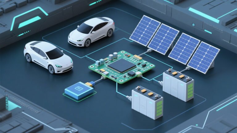
The PCB assembly process is a comprehensive manufacturing method that transforms bare printed circuit boards into fully functional electronic devices. Moreover, this process involves mounting electronic components onto PCB surfaces using advanced soldering techniques and automated equipment.
Furthermore, the PCB assembly process serves as the backbone of modern electronics manufacturing. In fact, every electronic device you use daily – from smartphones to automotive systems – relies on precise PCB assembly techniques. Additionally, this process ensures that electronic components work together seamlessly to create reliable products.
“The PCB assembly process has evolved from manual soldering to highly automated systems, reducing defect rates from 5% to less than 0.1% in modern facilities.” – Circuits Assembly Magazine
Key benefits of professional PCB assembly include:
- Higher Reliability: Automated processes reduce human error significantly
- Cost Efficiency: Mass production capabilities lower per-unit costs
- Quality Consistency: Standardized procedures ensure uniform results
- Faster Time-to-Market: Streamlined workflows accelerate product development
How is a Bare PCB Fabricated Before Assembly Begins?
Before electronic components are mounted, the journey starts with fabricating the bare printed circuit board itself—a crucial foundation for any assembly process.
Here’s how the bare PCB comes to life:
- Material Selection: The process kicks off by choosing a high-quality base material, most often FR4 fiberglass, layered with thin sheets of copper. This combination provides both structural integrity and excellent electrical pathways.
- Transferring the Circuit Pattern: Advanced photolithography techniques (think of it as high-tech “printing”) are used to etch the intended circuit layout onto the copper surface, ensuring precise pathway formation for future signals.
- Etching: Unwanted copper is chemically removed, leaving behind only the desired copper traces that will connect all components together.
- Drilling: Automated drills punch precise holes for through-hole components and vias, which enable interlayer connections.
- Copper Plating: An additional copper layer is electroplated onto the drilled holes, guaranteeing robust electrical connectivity between layers and mechanically reinforcing the structure.
- Applying Solder Mask and Silkscreen: Finally, a protective solder mask is coated over the traces to prevent accidental solder bridges during assembly, while a silkscreen layer adds valuable reference markings and polarity indicators.
By the end of this fabrication sequence, you’ve got a clean, feature-rich bare PCB—ready for component population and the next stage of assembly.
What is Single-Side Assembly? [Applications & Advantages]
Single-side assembly refers to the process where all electronic components are mounted exclusively on one side of a printed circuit board. This approach represents the simplest and most economical method in PCB assembly, making it ideal for projects where circuit complexity is low and budgets are tight.
You’ll commonly find single-side assembly used in devices such as basic calculators, LED lighting panels, remote controls, and simple toys. Since only one side of the board is populated with components, it naturally limits both the density and complexity of circuits you can create. However, for high-volume production of straightforward electronics, single-sided assembly remains the go-to choice due to:
- Lower production costs: Fewer layers and simpler processes keep expenses minimal.
- Faster assembly: Streamlined steps speed up manufacturing timelines.
- Reliable performance: Fewer solder joints mean fewer potential points of failure.
In summary, single-side PCB assembly is chosen when a design calls for efficiency, simplicity, and cost-effectiveness—making it highly relevant for everyday, mass-market consumer electronic products.
7-Step PCB Assembly Process (Step-by-Step Guide)
Understanding the complete PCB assembly process helps engineers and manufacturers optimize their production workflows. Consequently, let’s explore each critical step in detail.
Step 1: Design Verification and File Preparation
Initially, the PCB assembly process begins with thorough design verification. During this phase, engineers review Gerber files, Bill of Materials (BOM), and assembly drawings. Subsequently, Design for Assembly (DFA) analysis identifies potential manufacturing challenges before production starts.
Pro Tip: Proper DFA can reduce assembly time by up to 30% and minimize defect rates significantly.
Essential verification steps include:
- Gerber file accuracy validation
- Component availability confirmation
- Assembly drawing review
- Pick and place program creation
Step 2: Solder Paste Application
Next, the solder paste application phase uses precision stencils to deposit solder paste onto PCB pads. Meanwhile, 3D Solder Paste Inspection (SPI) systems verify paste volume, height, and alignment before component placement.
Professional stencil printing ensures precise solder paste application
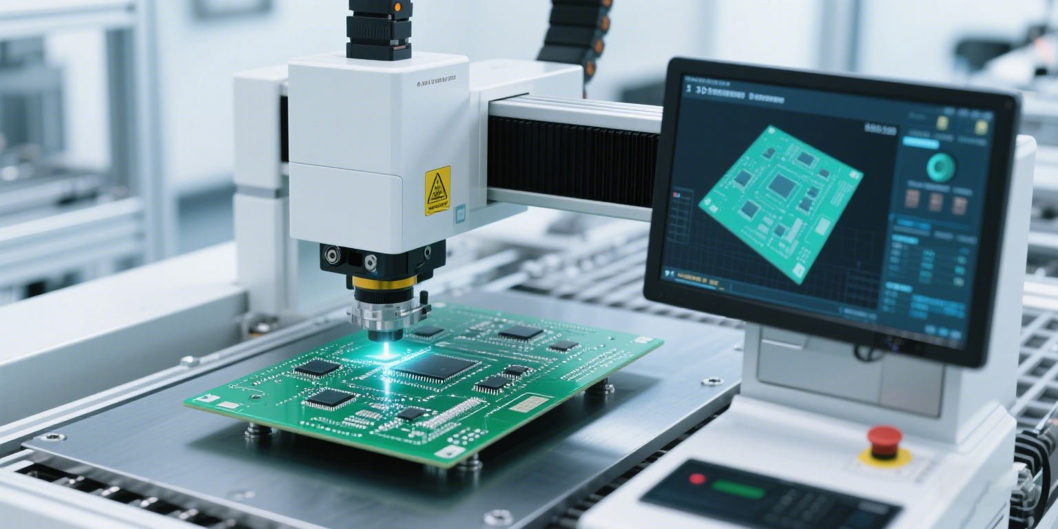
3D SPI systems verify solder paste quality before component placement
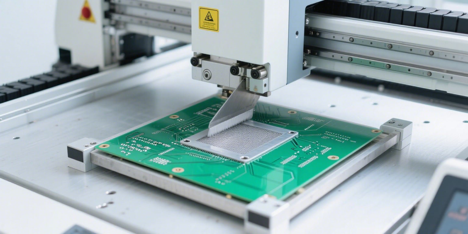
Step 3: Component Placement (SMT Assembly)
Subsequently, automated pick and place machines position surface-mount components with incredible precision. These machines can place thousands of components per hour while maintaining accuracy within ±0.05mm tolerances.
Modern SMT assembly handles various component types:
- Ultra-fine pitch components: 01005 packages and smaller
- Ball Grid Arrays (BGA): High-density interconnect solutions
- Quad Flat No-leads (QFN): Compact surface-mount packages
- System-in-Package (SiP): Advanced integrated modules
Leveraging IC Packages to Simplify Designs and Lower Costs
Selecting integrated circuit (IC) packages is a strategic way to streamline your PCB assembly. By incorporating ICs—such as microcontrollers, op-amps, or ASICs—you can effectively combine the functions of multiple discrete components into a single device. This reduction in total part count not only simplifies your circuit layout but also brings several production advantages:
- Lower Assembly Costs: Fewer individual components mean less placement time and reduced labor during assembly.
- Improved Reliability: Integrating functions into one IC minimizes the potential points of failure, contributing to greater long-term durability.
- Space Efficiency: ICs often enable more compact designs, freeing up valuable PCB real estate for additional features or smaller product footprints.
Tip: While ICs offer these advantages, always consider factors like ease of repair and long-term component sourcing. In some cases, highly specialized ICs may be harder to replace or upgrade compared to commonly available discrete parts. Balancing integration with serviceability ensures both cost-effectiveness and maintainability in your design.
Step 4: Reflow Soldering
Following component placement, reflow ovens use controlled temperature profiles to melt solder paste and create permanent connections. Furthermore, precise temperature control prevents component damage while ensuring reliable solder joints.
According to SMT NET, proper reflow profiling reduces solder defects by up to 85% compared to manual processes.
Step 5: Through-Hole Assembly (if needed)
Additionally, some PCB designs require through-hole components for enhanced mechanical strength. Therefore, wave soldering or selective soldering processes secure these components after SMT assembly completion.
Step 6: Inspection and Testing
Then, comprehensive inspection procedures verify assembly quality using multiple technologies:
- Automated Optical Inspection (AOI): Detects component placement issues
- X-Ray Inspection: Identifies hidden solder joint defects
- In-Circuit Testing (ICT): Verifies electrical connectivity
- Functional Circuit Testing (FCT): Confirms operational performance
Flying Probe Testing (FPT): Purpose and Advantages
Another critical inspection method is Flying Probe Testing (FPT). This automated electrical test evaluates for shorts, opens, and verifies key component values directly on the assembled PCB, without requiring a custom test fixture.
Advantages of FPT include:
- Ideal for Low-Volume Production: Unlike traditional in-circuit test fixtures, FPT doesn’t require custom tooling, making it especially cost-effective for prototypes and small batch runs.
- Flexible Test Coverage: Flying probes can access virtually any test point on the board, even in densely populated or complex designs.
- Rapid Setup: With minimal setup time, FPT supports faster transitions between projects—perfect for R&D and New Product Introduction (NPI).
- Comprehensive Diagnostics: The test identifies a wide range of defects, from solder bridges to missing components, ensuring robust assembly quality.
By integrating FPT, manufacturers can efficiently validate the electrical integrity of each PCB, safeguarding performance—especially in fast-paced or development-focused production environments.
Step 7: Final Quality Control
Finally, rigorous quality control procedures ensure every assembled PCB meets specifications. Moreover, First Article Inspection (FAI) documentation provides traceability for critical applications like automotive and medical devices.
SMT vs Through-Hole Assembly: Key Differences
Understanding the differences between SMT and through-hole assembly helps optimize the PCB assembly process for specific applications. Consequently, here’s a detailed comparison:
| Aspect | SMT Assembly | Through-Hole Assembly |
|---|---|---|
| Component Size | Smaller, more compact | Larger with leads |
| Assembly Speed | High-speed automated | Slower, may require manual steps |
| Mechanical Strength | Lower mechanical bond | Stronger mechanical connection |
| PCB Space Utilization | Both sides available | Limits component placement |
| Cost Efficiency | Lower for high volumes | Higher due to drilling costs |
| Rework Difficulty | More challenging | Easier component replacement |
Furthermore, modern PCB assembly processes often combine both technologies to leverage their respective advantages. For instance, SMT components handle most circuit functions while through-hole components provide mechanical stability for connectors and power components.
Double-Sided Mixed Assembly: An Overview
Double-sided mixed assembly refers to the technique of mounting both surface-mount and through-hole components on both sides of a single PCB. This approach delivers maximum flexibility for engineers, allowing them to optimize circuit density and functionality by selecting the best component type for each specific location—regardless of which PCB surface is available.
Designers often rely on double-sided mixed assembly when faced with demanding applications, such as compact industrial controllers, network routers, or sophisticated consumer electronics where valuable board space is extremely limited. However, the increased complexity in both assembly and inspection means that projects using this method may experience higher production costs and longer lead times.
Despite these challenges, combining SMT and through-hole technologies on both sides of the board remains critical for advanced products requiring robust mechanical connections alongside dense, miniaturized circuits.
What Is Single-Sided Mixed Assembly—and When Does It Make Sense?
Single-sided mixed assembly refers to the practice of mounting both through-hole and surface-mount (SMT) components on only one side of the printed circuit board. This hybrid approach is particularly useful when your design calls for a few specific through-hole parts—such as connectors or high-stress components—but you want to retain the space savings and efficiency of SMT for the rest of the circuitry.
When does this technique shine?
- Board space is at a premium: You need to pack in as much functionality as possible without turning to a double-sided build.
- Design simplification: By restricting all components to one side, manufacturing complexity and costs are kept in check.
- Mechanical reliability: Essential through-hole parts deliver durability where it matters, while SMT maximizes space for signal processing and smaller ICs.
Ultimately, single-sided mixed assembly is a smart compromise that balances robust mechanical connections and efficient use of PCB real estate. This approach is commonly seen in cost-sensitive designs or where manufacturability and reliability must both be considered.
PCB Assembly Equipment and Technologies
Advanced equipment drives efficiency improvements in the PCB assembly process. Meanwhile, automation technologies continue revolutionizing manufacturing capabilities.
Automated Pick and Place Machines
Modern pick and place systems achieve placement rates exceeding 100,000 components per hour. Additionally, vision systems ensure accurate component orientation and position verification.
ROI Insight: High-speed pick and place machines typically pay for themselves within 18-24 months through increased productivity and reduced labor costs.
Advanced Inspection Technologies
Moreover, inspection equipment evolution significantly improves defect detection capabilities:
- 3D SPI Systems: Measure solder paste volume with 99.9% accuracy
- X-Ray Inspection: Detect hidden BGA and QFN solder defects
- Automated Optical Inspection: Identify component placement issues instantly
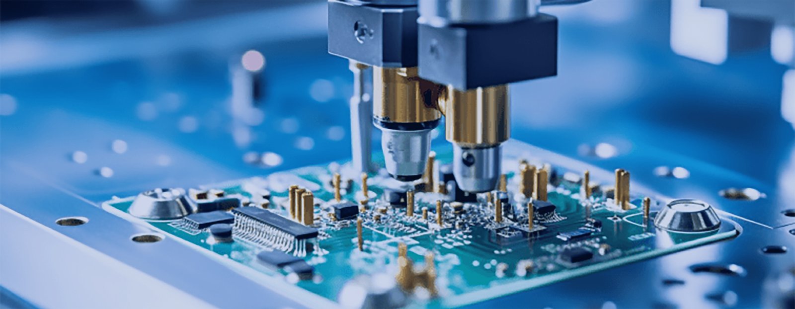
High-speed pick and place machines ensure precise component placement


Common PCB Assembly Challenges (And How to Avoid Them)
Despite technological advances, the PCB assembly process faces several recurring challenges. However, understanding these issues enables proactive prevention strategies.
Challenge 1: Component Miniaturization Issues
Increasingly smaller components create placement and inspection difficulties. Nevertheless, advanced vision systems and precision placement equipment address these challenges effectively.
Solutions:
- Upgrade to high-resolution vision systems
- Implement 3D inspection technologies
- Use specialized nozzles for tiny components
- Optimize stencil design for fine-pitch components
Challenge 2: Solder Defects and Quality Issues
Common solder defects include bridges, insufficient paste, and tombstoning. Fortunately, proper process control and inspection prevent most quality issues.
“Implementing 3D SPI reduced our solder-related defects by 78% within the first quarter of deployment.” – Manufacturing Quality Manager, Electronics Manufacturing
Challenge 3: Supply Chain and Component Availability
Component shortages significantly impact the PCB assembly process timeline. Therefore, proactive supply chain management becomes critical for success.
Best Practices:
- Maintain strategic component inventory
- Develop multiple supplier relationships
- Implement alternative component strategies
- Use predictive analytics for demand planning
Leveraging Your Own Supply Chain During PCB Assembly
For organizations seeking greater oversight or cost optimization, many PCB assembly providers offer partially consigned assembly options. This approach allows customers to take an active role in the supply chain by supplying select components—especially those that are proprietary, high-value, or sourced through preferred vendors like Mustar.
Key benefits include:
- Direct Component Control: Choose specialty or custom parts to ensure the desired quality, authenticity, and performance.
- Cost Management: Avoid markup on component costs by purchasing directly from trusted distributors or in larger volumes for future use.
- Risk Mitigation: Minimize delays or shortages by securing critical or long-lead-time components through your established channels.
The assembly partner then handles the remaining aspects—including PCB fabrication, sourcing of standard components if needed, and the full assembly process—ensuring a seamless transition from supply chain management to manufacturing execution.
This flexible strategy empowers project managers and engineers alike to balance reliability, speed, and budget requirements across a wide range of applications.
PCB Assembly Market Trends and Future Outlook
The global PCB assembly process market continues expanding rapidly, driven by technological innovations and increasing electronics demand. Furthermore, several key trends shape industry development.
Market Growth Statistics
| Metric | 2023 Value | 2032 Projection | Growth Rate |
|---|---|---|---|
| Global Market Size | $9.1 Billion | $21.46 Billion | 10% CAGR |
| Asia Pacific Share | 60% | 65% | Increasing |
| Automotive Segment | 25% share | 30% share | 12% CAGR |
| Medical Electronics | 15% share | 18% share | 8% CAGR |
Data source:dataintelo verifiedmarketresearch
Key Growth Drivers
Several factors accelerate PCB assembly process market expansion:
- 5G Technology Deployment: Drives demand for high-frequency PCBs
- Electric Vehicle Growth: Increases automotive electronics requirements
- IoT Device Proliferation: Expands consumer electronics market
- Medical Device Innovation: Creates specialized assembly needs
According to Grand View Research, the automotive PCB assembly segment shows the highest growth potential, with electric vehicles requiring 3-5 times more PCBs than traditional vehicles.
Emerging Technology Trends
Additionally, several technological developments reshape the PCB assembly process:
- Artificial Intelligence Integration: Predictive maintenance and quality optimization
- Flexible PCB Adoption: Wearable devices and compact electronics
- Advanced Materials: High-frequency and thermal management solutions
- Industry 4.0 Implementation: Smart factory automation and data analytics
Choosing the Right PCB Assembly Partner
Selecting an experienced PCB assembly partner significantly impacts product quality and time-to-market success. Therefore, several critical factors deserve careful evaluation.
Essential Certification Requirements
Professional PCB assembly process providers maintain multiple industry certifications:
- ISO 9001: Quality management systems
- IATF 16949: Automotive quality standards
- ISO 13485: Medical device manufacturing
- IPC Standards: Electronics assembly best practices
- RoHS Compliance: Environmental regulations
Advanced Manufacturing Capabilities
Moreover, leading assembly partners offer comprehensive capabilities:
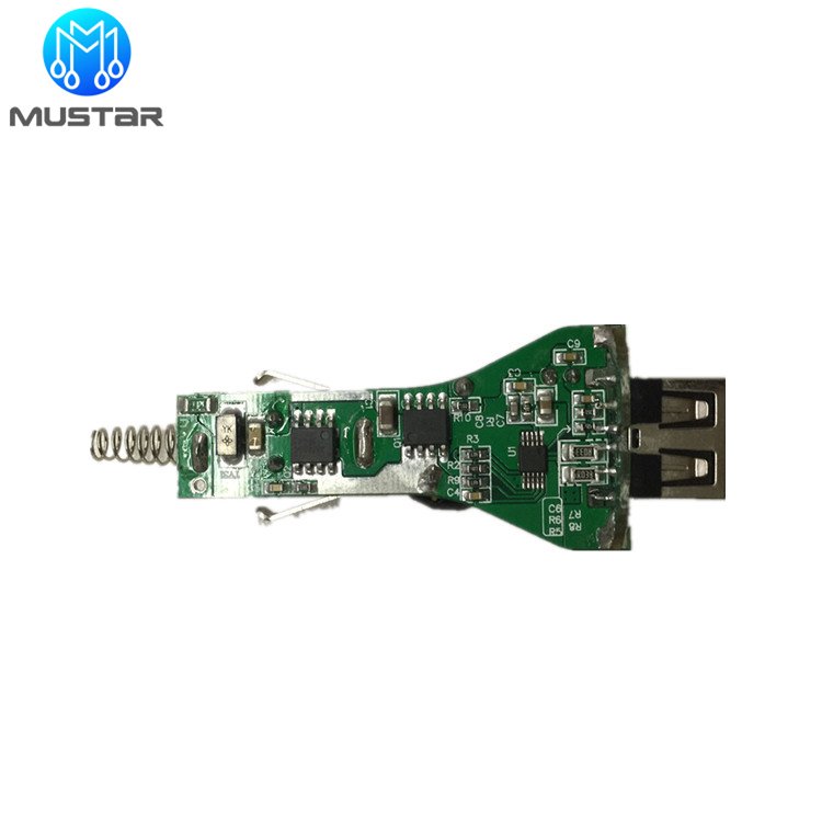
Example: Mustar, a leading PCB assembly manufacturer, provides turnkey solutions including 64-layer PCB fabrication, 01005 component placement, and specialized automotive/medical production lines with over 25 years of industry experience.
- Multi-layer PCB assembly (up to 64 layers)
- Ultra-fine pitch component handling
- Advanced inspection and testing capabilities
- Global component sourcing networks
- Fast prototype to production scaling
Supply Chain Strength
Furthermore, robust supply chain management ensures component availability and cost optimization. Professional partners maintain relationships with 200+ global suppliers while providing alternative sourcing strategies.
For more insights on electronics manufacturing trends, visit Assembly Magazine for industry updates and technical resources.
Ready to Optimize Your PCB Assembly Process?
Don’t let assembly challenges slow down your product development. Partner with experienced professionals who understand the complexities of modern PCB assembly and can deliver the quality your projects demand.
Get started today with a trusted PCB assembly partner:
- ✅ Free DFA (Design for Assembly) review
- ✅ Competitive pricing with transparent quotes
- ✅ Fast prototyping (4-8 hours for samples)
- ✅ Full certification compliance (ISO, IATF, IPC)
- ✅ 25+ years of proven assembly experience
Get Your Free Quote Today
View Our Capabilities
Contact Mustar Company: Ready to discuss your PCB assembly requirements? Our experienced team provides personalized solutions for automotive, medical, and industrial applications.
Mustar projects