Overview of PCB Packaging Technologies: Definitions and Development of SMD, THT, and BGA
PCB (Printed Circuit Board) packaging technologies primarily include SMD (Surface Mount Device), THT (Through-Hole Technology), and BGA (Ball Grid Array). SMD mounts components directly on the PCB surface using automated machines, enabling miniaturization and mass production of electronic devices. THT requires inserting component leads through drilled holes in the PCB, offering strong mechanical stability and suitability for high power applications. BGA features a grid of solder balls underneath the component, providing excellent electrical performance and heat dissipation, making it ideal for high-end chips and complex modules.
Latest Market Share and Application Data for SMD, THT, and BGA Technologies
-
In 2023, SMD packaging accounted for 90.3% market share in the small-pitch LED display market in China.
-
Through-hole THT packaging held approximately 26.5% of the market, commonly used in power electronics, automotive, and industrial control.
-
The global BGA substrate market reached $7.02 billion in 2024, with a projected compound annual growth rate (CAGR) of 6.2%, expected to hit $10.63 billion by 2031.
| Packaging Technology | 2023 Market Share | Main Application Areas | Typical Advantages |
|---|---|---|---|
| SMD | 90.3% | Consumer electronics, LED, small PCB circuits | Highly automated, compact, suitable for mass production |
| THT | 26.5% | Power supplies, automotive electronics, industrial controls | Strong mechanical strength, heat resistant |
| BGA | $7 billion market | High-performance computing, CPUs, GPUs | Numerous solder joints, excellent heat dissipation and signal integrity |
Comparative Analysis of Advantages and Disadvantages
-
SMD: Small package size and high automation level; suitable for high-density PCBs. However, repair and manual replacement are relatively complex.
-
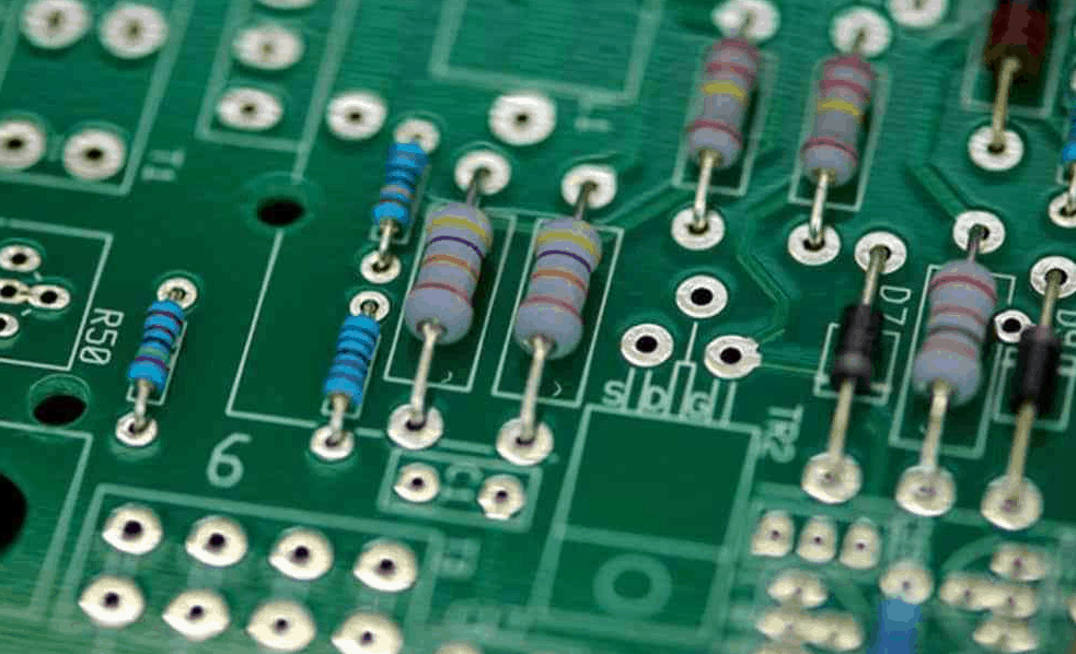
THT: High mechanical strength and heat resistance; ideal for high current and high impact scenarios. But has lower routing density and increases PCB size.
-
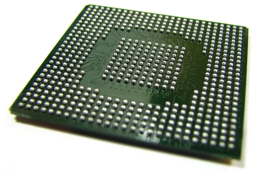
BGA: Supports high pin count and high performance, with superior electrical and thermal properties. However, solder joints are not visible, making inspection and repair difficult.
How to Choose the Right PCB Packaging Technology for Your Project
Select the packaging technology based on factors including application environment (vibration, temperature), electrical performance, production cost, volume, and maintenance convenience. For example, projects with high reliability and current demands favor THT; space-saving and automated production scenarios suit SMD; complex signal processing and high-performance modules typically require BGA.
Industrial Case Studies: Typical Applications of Mainstream Packaging Technologies
-
SMD is widely used in smartphones, TVs, laptops, and other consumer electronics.
-
THT is preferred in automotive controllers, industrial power supplies, and other high-stress environments.
-
BGA is the mainstream choice for high-performance computing modules like CPUs, GPUs, and data center server motherboards.
Common Design and Manufacturing Pitfalls When Choosing Packaging
Errors such as incorrect library choices, improper pad layout, and inadequate solder pad size or spacing can directly affect product reliability and manufacturability.
Future Trends: Advancement of BGA, High-Density Interconnects, and New Packaging Techniques
Automation and design density continue to increase, with advanced packaging technologies (like higher-density BGA and fan-out packages) gaining market share. Reliability and thermal management remain critical focus areas.
Mustar offers professional full-process PCB packaging selection, prototyping, and mass production services to help efficiently realize your complex projects.
For customized PCB prototyping, bulk manufacturing, or more detailed technical solutions, please contact Mustar’s engineering team.
Mustar projects: