
Contents
- Market at a Glance (2025)
- Introduction to PCB Assembly
- Key Components and Materials Used in PCB Assembly
- The PCB Assembly Process Explained
- Types of PCB Assembly Technologies
- Quality Control in PCB Assembly
- Factors Affecting PCB Assembly Cost
- Market Trends and Industry Statistics
- Challenges and Innovations in PCB Assembly
- Why Choose Mustar for Your PCB Assembly Needs
- Conclusion
PCB Assembly Market at a Glance (2025)
| Metric | Data / Statistic |
|---|---|
| Global PCB Assembly Market Size | Over USD 90 billion in 2023 |
| Market Growth (2023-2032) | Approximately 5% CAGR |
| Expected Market Growth (2025-2029) | USD 26.8 billion |
| Leading Assembly Technology | Surface Mount Technology (SMT) – 30%+ market share |
| Typical PCB Assembly Cost | $0.15 to $0.30 per piece (assembly and testing) |
Introduction to PCB Assembly
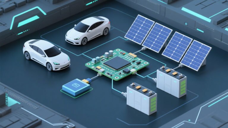
PCB Assembly (PCBA) is the process of mounting electronic components onto a bare printed circuit board to create a functional electronic circuit. In fact, this crucial manufacturing step transforms an empty PCB into a working electronic device that powers everything from your smartphone to medical equipment.
Without proper PCB assembly, even the best-designed circuit boards would remain useless. Moreover, as electronics continue to evolve and become more compact, the assembly process has become increasingly sophisticated and precise.
“PCB Assembly is the backbone of modern electronics manufacturing, bridging design concepts to functional devices through precise component placement and soldering techniques.”
Let’s explore why PCB assembly matters so much in today’s electronics industry and how it brings your devices to life.
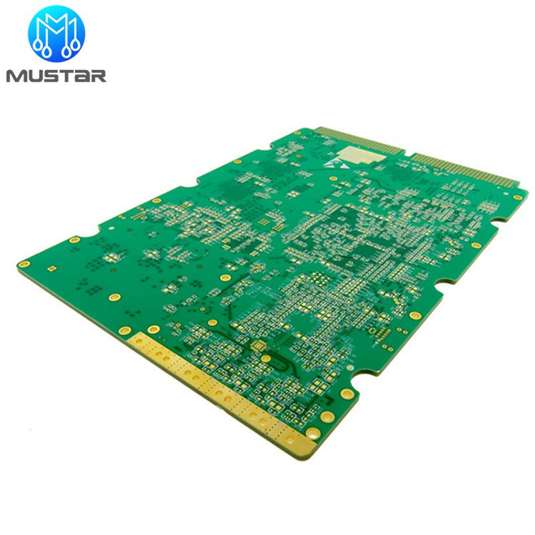
A bare PCB before component assembly
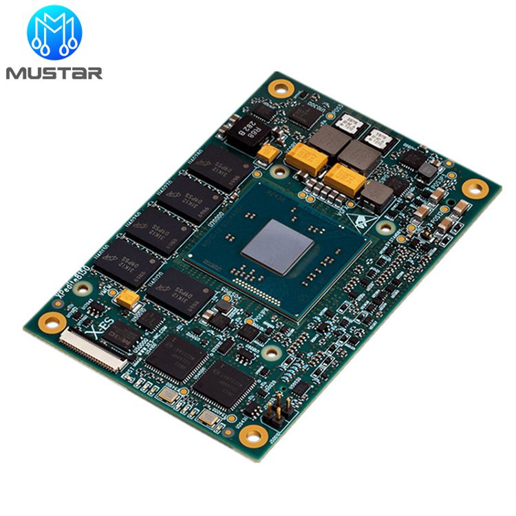
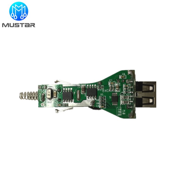
A fully assembled PCB with components mounted
Key Components and Materials Used in PCB Assembly
The quality and reliability of a PCBA depend heavily on the components and materials used. Therefore, understanding these elements is essential for anyone involved in electronics manufacturing.
Common Electronic Components
- Resistors: Control current flow within the circuit
- Capacitors: Store and release electrical energy
- Integrated Circuits (ICs): Perform specific functions, essentially the “brains” of the device
- Transistors: Amplify or switch electronic signals
- Diodes: Allow current to flow in one direction only
- Connectors: Provide interfaces to other devices or power sources
Essential Materials
Besides components, several key materials are vital to the PCB assembly process:
- Copper: Forms the conductive pathways on the PCB
- Fiberglass: Provides the rigid structure and insulation (FR-4 is commonly used)
- Solder: Typically lead-free alloys that create electrical connections
- Solder Mask: The green (or other colored) layer that protects copper traces
- Silkscreen: Printed text and symbols that help with component identification
The selection of these materials significantly impacts the performance standards and durability of the final assembled PCB.
The PCB Assembly Process Explained
Understanding the step-by-step PCB assembly process helps you appreciate the precision and care that goes into creating reliable electronic devices. Furthermore, each stage requires specialized equipment and expertise to ensure quality results.
1. Solder Paste Application
The assembly process begins with applying solder paste to the bare PCB:
- A stencil is perfectly aligned over the board
- Solder paste (tiny metal particles in flux) is spread across the stencil
- The stencil is removed, leaving precise deposits of paste only on the pads
- Quality control measures like Solder Paste Inspection (SPI) verify correct application
2. Component Placement
Next, components are precisely positioned on the board:
- SMT (Surface Mount Technology): Components are placed directly onto the solder paste
- Through-hole: Component leads are inserted through pre-drilled holes
- Pick-and-place machines achieve placement accuracy down to 0.01mm
- Advanced vision systems ensure correct positioning
3. Soldering Methods
Once components are placed, they must be permanently attached to the PCB:
- Reflow Soldering: The entire board passes through a reflow oven with controlled temperature zones, melting the solder paste to form permanent connections
- Wave Soldering: Primarily used for through-hole components, where the bottom of the board contacts a wave of molten solder
- Selective Soldering: Used when only specific areas need soldering
- Hand Soldering: For specialized components or repairs
4. Inspection and Testing
After soldering, rigorous inspection and testing ensure functionality:
- Automated Optical Inspection (AOI): High-resolution cameras identify soldering defects
- X-Ray Inspection: Verifies hidden connections like those under BGA components
- In-Circuit Testing (ICT): Electrical tests confirm component functionality
- Functional Circuit Testing (FCT): Ensures the assembled PCB performs as designed
- First Article Inspection (FAI): Thorough examination of initial production units
This multi-stage assembly process ensures that every PCB meets quality and performance requirements.
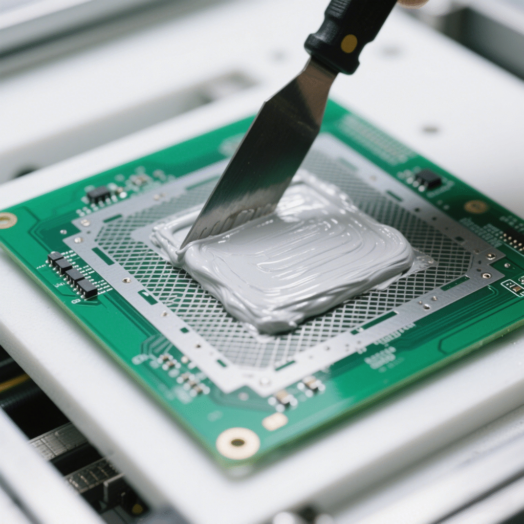
Precise solder paste application through stencil
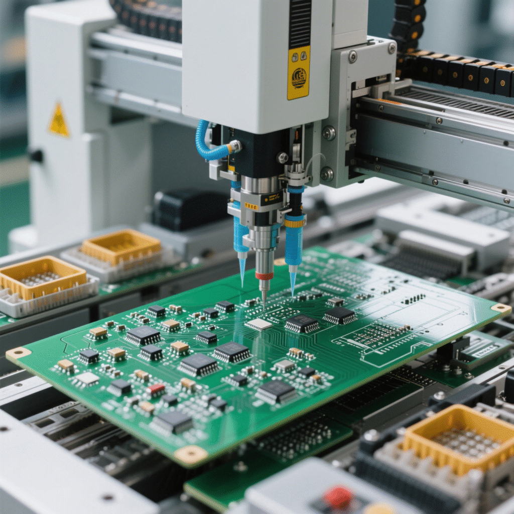
High-speed pick-and-place machine mounting components
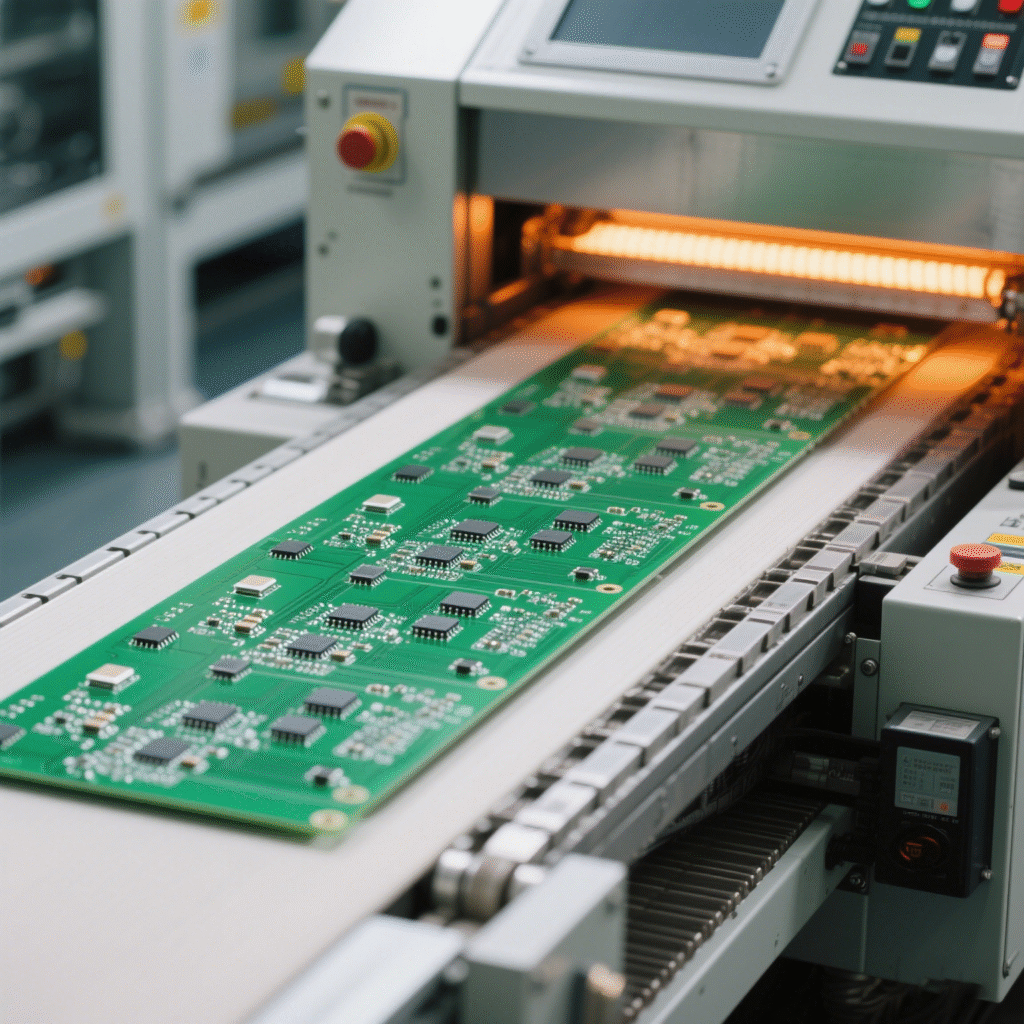
PCB moving through reflow oven zones
Types of PCB Assembly Technologies
Different assembly technologies serve various requirements for electronic devices. In addition, the choice of technology affects cost, reliability, and production speed.
Types of PCB Assembly Services
Choosing the right PCB assembly service depends on your project’s requirements, timelines, and level of control you want over sourcing. Generally, PCB assembly services fall into three common categories:
1. Full Turnkey Assembly
In a full turnkey assembly, the manufacturing partner manages the process from start to finish. This includes:
- PCB fabrication according to your specifications
- Acquisition of all electronic components
- Complete assembly of the board
- Comprehensive testing and inspection
- Final packaging and shipping
Full turnkey is ideal for those seeking a seamless, all-in-one solution—especially helpful when speed and convenience are critical, or if you prefer not to juggle multiple vendors.
2. Partial Turnkey (or Partial Consignment) Assembly
Partial turnkey services provide more flexibility if you’d like to supply some of your own components, such as specialized chips or hard-to-source parts. In this model:
- You source and provide selected components
- The assembler handles the rest, including PCB manufacturing and remaining parts procurement
- Assembly and quality control are performed as usual
This approach allows you to exercise greater control over certain aspects of sourcing, often resulting in cost savings or component preference while still enjoying professional assembly support.
3. Consigned Assembly
Consigned or contractor assembly places most of the responsibility for component sourcing on you. Here’s how it works:
- You supply all components and the bare PCB
- The assembler focuses solely on putting everything together
Consigned assembly is well-suited for projects where you already have established suppliers or strict requirements for specific parts and substrates. It allows for maximum oversight on component quality and origin, while leveraging experienced assemblers for precise manufacturing.
Understanding these service types can help you choose the best partner and workflow for your next electronics project, whether you value convenience, control, or a blend of both.
Surface Mount Technology (SMT)
SMT has revolutionized electronics manufacturing since its widespread adoption in the 1980s:
- Components mount directly onto the PCB surface
- Allows for much higher component density
- Supports miniaturization of electronic devices
- Typically faster and more automated than through-hole
- Handles components as small as 01005 (0.4mm × 0.2mm)
Through-Hole Technology (THT)
Though older, THT remains important for specific applications:
- Component leads insert through holes in the PCB
- Provides stronger mechanical bonds for high-stress environments
- Better for high-power components that generate significant heat
- Often used in military and aerospace applications where reliability is critical
Double-Sided PCB Assembly
Double-sided PCB assembly involves mounting electronic components on both the top and bottom surfaces of a single board. This technology makes it possible to create more sophisticated circuits without increasing the overall board size.
Benefits of Double-Sided Assembly include:
- Greater Component Density: By utilizing both sides, engineers can fit more connections and features into compact spaces—ideal for modern gadgets and devices.
- Design Flexibility: Makers can mix and match surface mount and through-hole components, giving added versatility for complex circuit designs.
- Cost Efficiency in Compact Projects: Rather than expanding the footprint, double-sided PCBs help save space and potentially lower costs for certain designs.
- Support for Complex Functionality: Many advanced electronics, from smartphones to industrial controls, rely on double-sided assemblies for the increased circuitry they require.
Though the process is more intricate than assembling single-sided boards, the payoff is well worth it for products demanding high performance in a small package.
Mixed Technology and Advanced Methods
Many modern PCBs utilize a combination of technologies:
- Mixed Technology: Combines SMT and THT on the same board
- Ball Grid Array (BGA): Uses an array of solder balls beneath components for high-density connections
- Chip-Scale Packaging (CSP): Nearly the same size as the silicon die inside
- Flip Chip: Dies are flipped and connected directly to the substrate
According to industry reports, SMT now dominates with over 30% of the global market share due to its efficiency and compatibility with automation.
Quality Control in PCB Assembly
Quality control is absolutely essential in PCB assembly, especially for applications where failure is not an option. Additionally, proper quality processes save money by reducing rework and warranty claims.
Inspection Techniques and Testing
Comprehensive quality control employs multiple inspection methods:
- 3D Solder Paste Inspection (SPI): Verifies correct solder paste volume and position
- Automated Optical Inspection (AOI): Cameras detect missing components, incorrect orientation, and solder defects
- 3D X-Ray Inspection: Reveals hidden joints under components like BGAs
- In-Circuit Testing (ICT): Electrical tests using “bed of nails” fixtures verify component functionality
- Flying Probe Testing: More flexible alternative to ICT for lower volumes
- Functional Testing: Confirms the circuit performs as designed under actual operating conditions
Statistical Process Control (SPC)
Beyond individual board testing, SPC monitors the manufacturing process itself:
- Collects and analyzes data to identify trends
- Detects process shifts before they cause quality issues
- Reduces defects by maintaining process stability
- Documentation helps with traceability and continuous improvement
Environmental Testing and Compliance
Finished PCBAs often undergo environmental testing to ensure reliability:
- Thermal Cycling: Tests performance through temperature extremes
- Vibration Testing: Verifies durability in high-vibration environments
- Humidity Testing: Ensures resistance to moisture
- Compliance Testing: Confirms adherence to standards like RoHS, REACH, and industry-specific requirements
These quality control measures are particularly important for PCBAs used in critical applications like automotive safety systems, medical devices, and aerospace equipment.
Factors Affecting PCB Assembly Cost
Understanding cost factors helps you make informed decisions when planning your electronics projects. Moreover, cost optimization doesn’t have to mean sacrificing quality.
Breakdown of Cost Components
PCB assembly costs include several elements:
- PCB Production: The bare board itself (10-30% of total cost)
- Components: Often the largest expense (40-60% of total cost)
- Labor: Varies significantly by region and automation level
- Testing: More comprehensive testing increases costs but improves reliability
- Setup and NRE: One-time engineering costs spread across production volume
Key Cost Drivers
Several factors significantly impact final assembly costs:
- Volume: Higher quantities generally reduce per-unit costs
- Component Selection: Using common components reduces sourcing costs
- Design Complexity: More layers and components increase costs
- Technology Requirements: Advanced technologies like micro-BGAs cost more
- Turnaround Time: Rush orders command premium prices
- Quality Requirements: Higher reliability standards increase testing costs
| Volume | Typical Assembly Cost Range (per board) |
|---|---|
| Prototype (1-10 units) | $10-$50+ |
| Small Run (10-500 units) | $5-$20 |
| Medium Production (500-5,000) | $1-$10 |
| High Volume (5,000+) | $0.15-$5 |
For a deeper analysis of PCB assembly costs, industry cost guides provide valuable benchmarks for budgeting.
Market Trends and Industry Statistics
The PCB assembly market continues to evolve rapidly. Furthermore, understanding these trends helps businesses stay competitive and plan for future technology needs.
Global PCB Assembly Market Size and Growth
The PCBA market shows strong growth prospects:
- Global market exceeded USD 90 billion in 2023
- Expected growth of USD 26.8 billion between 2025-2029
- Compound Annual Growth Rate (CAGR) of approximately 5-6.2%
- Automotive and consumer electronics driving significant demand
Regional Manufacturing Hubs
Production continues to shift globally:
- Asia Pacific: Dominates with over 25% market share, led by China, Taiwan, and Vietnam
- North America: Focuses on high-reliability, defense, and medical applications
- Europe: Specializes in automotive and industrial electronics
- Emerging Markets: Countries like Mexico, India, and Eastern Europe gaining market share
Technology Trends Driving Growth
Several technologies are reshaping PCB assembly:
- Artificial Intelligence (AI): Increasing demand for specialized high-performance PCBAs
- Internet of Things (IoT): Driving need for compact, energy-efficient boards
- 5G Technology: Requiring advanced high-frequency PCB designs
- Electric Vehicles: Creating demand for high-power, high-reliability automotive PCBAs
- Wearable Devices: Pushing the boundaries of miniaturization
Industry analysts at Grand View Research predict continued growth in high-density interconnect (HDI) PCBs as devices become increasingly compact.
Challenges and Innovations in PCB Assembly
The PCB assembly industry faces several challenges while continuing to innovate. As a result, manufacturers must adapt to stay competitive in this rapidly evolving landscape.
Miniaturization and Complexity
As devices shrink, assembly becomes more challenging:
- Components now available in packages as small as 01005 (0.4mm × 0.2mm)
- Pin pitches decreasing to 0.3mm and below
- Higher component density requiring more precise placement
- Increased use of stacked packages and embedded components
- PCB layer counts increasing for complex designs
Automation and Smart Manufacturing
Industry 4.0 is transforming PCB assembly:
- Lights-Out Manufacturing: Fully automated production lines
- AI-Powered Inspection: More accurate defect detection
- Digital Twin Technology: Virtual simulation of the production process
- Real-Time Monitoring: Immediate process adjustments based on data
- Machine Learning: Continuous improvement of manufacturing parameters
Materials and Design Innovations
New materials address emerging challenges:
- High-Frequency Materials: Supporting 5G and other RF applications
- Thermal Management Solutions: For high-power applications
- Flexible and Rigid-Flex PCBs: Enabling new form factors
- Lead-Free Solder Alternatives: Improving reliability while meeting environmental regulations
- Embedded Components: Resistors and capacitors built into the PCB itself
For more insights on emerging PCB assembly technologies, industry publications provide regular updates on innovations.
Why Choose Mustar for Your PCB Assembly Needs
With so many PCB assembly providers available, Mustar stands out as an exceptional partner for your electronics manufacturing needs. In particular, our 25+ years of experience sets us apart from newer competitors.
Our Expertise and Capabilities
- Comprehensive Services: One-stop solution from PCB manufacturing to component sourcing and assembly
- Advanced Manufacturing: Production of complex PCBs up to 64 layers with cutting-edge technologies
- Specialized Production: Dedicated SMT lines for automotive and medical products
- Component Sourcing: Network of 200+ global suppliers with professional purchasing agents
- Rapid Prototyping: PCB sample production in as little as 4-8 hours
Quality Assurance
- Industry Certifications: ISO9001, ISO13485 (medical), ISO14001 (environmental), IATF16949 (automotive)
- Advanced Testing: ICT, FCT, 3D SPI, 3D X-Ray, AOI, and FAI ensuring product reliability
- Standardized Processes: Strict SOPs for consistent quality
- Proven Track Record: Successfully completing thousands of PCBA projects for demanding industries
Customer Service
- International Support: Over 100 international sales professionals
- Technical Expertise: 50+ component sourcing engineers providing technical assistance
- Customized Solutions: Tailored approach to each client’s unique requirements
- Transparent Communication: Regular updates throughout the manufacturing process
Our factory in Shenzhen, China spans approximately 12,000 square meters with over 600 staff dedicated to delivering high-quality PCB assembly services to clients worldwide.
Conclusion: Taking the Next Step in Your PCB Assembly Journey
PCB assembly is truly the backbone of modern electronics manufacturing, transforming bare circuit boards into functional electronic devices through precise component placement and soldering. As we’ve explored, the process involves sophisticated technology, rigorous quality control, and specialized expertise.
Whether you’re developing prototypes for a new product, scaling up production, or seeking more reliable manufacturing for your existing devices, choosing the right PCBA partner is crucial to your success. The right manufacturer can help optimize your designs, reduce costs, and ensure consistent quality.
At Mustar, we’ve been perfecting PCB assembly for over 25 years, serving industries from automotive to medical and new energy. Our comprehensive capabilities, stringent quality control, and customer-focused approach make us an ideal partner for your electronics manufacturing needs.
Ready to Start Your PCB Assembly Project?
Contact our expert team today for a consultation and quote. We’ll help you navigate the complexities of PCB assembly and find the most effective solution for your specific requirements.
Or call us directly: +86 136 8883 2535
Remember, the quality of your PCB assembly directly impacts the performance, reliability, and longevity of your electronic products. Don’t leave it to chance—partner with a proven expert in high-precision PCBA manufacturing.
Mustar projects: